How is the microelectronics industry maintaining its performance in the face of environmental challenges?
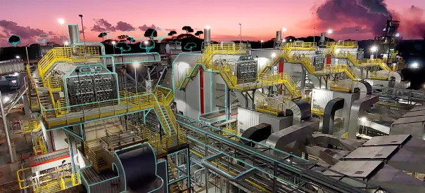
The microelectronics sector from semiconductor fabs to printed circuit board manufacturers operates at the intersection of extreme precision and massive resource consumption. As chip geometries shrink and wafer sizes grow, the demand for ultra-pure water, safe chemical waste disposal, and reliable energy supply intensifies. Manufacturers must simultaneously accelerate output, reduce their environmental footprint, and comply with increasingly stringent global regulations all without a single hour of unplanned downtime.
The global chip market is projected to surpass $1 trillion by 2030.*
Microelectronics industry challenges
Water intensity and purity demands
Microelectronics manufacturing is among the most water-intensive industries in the world. Producing a large integrated circuit on a 300 mm wafer requires approximately 8,300 liters of water, including nearly 5,700 liters of ultrapure water. As fabs continue to expand in regions facing increasing water stress, securing reliable, high-quality water supply has become a strategic imperative for operational resilience, production continuity, and future growth.
Energy and decarbonization: transition challenges
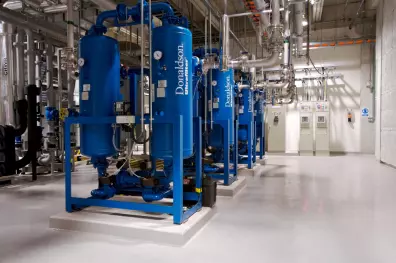
Semiconductor fabs are among the most energy-intensive industrial facilities in the world. In some facilities, electricity costs can represent up to 30% of operating expenses, highlighting the critical role of energy efficiency in maintaining competitiveness. The industry already generates 185 million tons of CO₂ equivalent emissions annually, and its footprint is expected to grow as global production expands. Improving energy performance and accelerating decarbonization have therefore become strategic priorities across the semiconductor value chain.
Hazardous waste and PFAS compliance
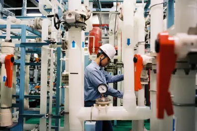
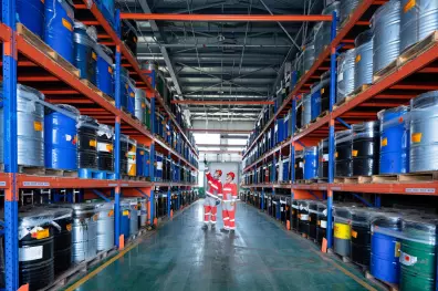
Semiconductor manufacturing generates some of the most complex industrial waste streams, including acids, solvents, metal-bearing residues, specialty chemicals, and emerging contaminants such as PFAS. As environmental regulations tighten and stakeholder expectations continue to rise, manufacturers face increasing pressure to ensure compliant, safe, and sustainable waste management. Optimizing treatment, recovery, and disposal strategies has become essential to reducing environmental risk, supporting circularity goals, and maintaining operational excellence.

Our tailored solutions for the microelectronics industry
How to make the microelectronics sector more resilient and sustainable?
Thanks to its expertise in water, waste and energy management, Veolia implements tailored solutions for the microelectronics industry to:
Guarantee operational continuity, by delivering reliable, uninterrupted ultra-pure water and energy supply through redundant systems, 24/7 expert monitoring, and rapid-response maintenance.
Lower costs and increase production efficiency, by optimizing water reuse rates, reducing energy consumption, and recovering valuable by-products from waste streams.
Ensure regulatory compliance and full traceability, by continuously adapting our solutions to evolving PFAS, TSCA, and environmental discharge regulations, with transparent digital reporting at every step.
Advance sustainability, by embedding circular economy principles across water recycling, solvent recovery, metals reclamation, and renewable energy integration, helping clients meet their net-zero and ESG commitments.
“ The semiconductor industry's resource demands are unlike any other. With water purity measured in parts per trillion, energy consumption rivalling small cities, and waste streams of extraordinary complexity, microelectronics manufacturers need partners who combine deep technical expertise with a genuine commitment to their operational success. That is exactly what we deliver — every day, on every site. ”
Ann Feng
Market Director, Microelectronics, Veolia
They did it!
United States of America
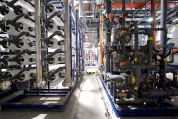
A high-tech electronics manufacturer in Texas implemented a custom ZLD water reuse system, achieving 95% process water reuse and generating an estimated $30 million in operational savings. The solution integrated advanced membrane technologies with digital monitoring capabilities, delivering both environmental performance and a compelling return on investment — demonstrating the tangible business case for water circularity in microelectronics.
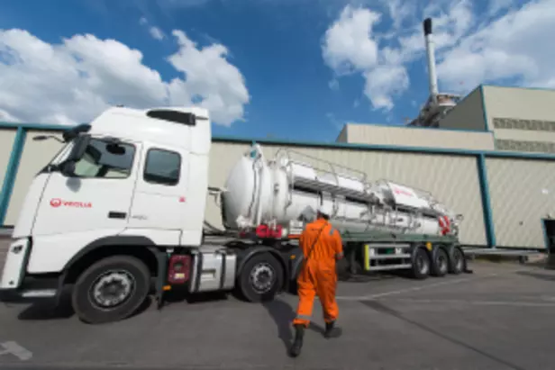
Across multiple European semiconductor manufacturing sites, we provide integrated hazardous waste management services covering PFAS-containing process chemicals, spent solvents, and complex etchant waste streams. Leveraging its network of certified treatment and incineration facilities — with 99.99% destruction efficiency — we ensure clients remain ahead of tightening EU PFAS regulations while recovering value from waste through solvent recycling and metals reclamation programmes.

Singapore
STMicroelectronics, a major player in 12-inch wafer production in Singapore, was facing growing demand in the semiconductor industry. To meet this demand, the company needed a new water treatment plant capable of supplying reliable ultrapure water, essential for the quality of 200 mm wafers. The project was completed in just four months, from contract award to water certification. It included the design, construction and commissioning of a new ultrapure water treatment plant, with a capacity of 160 m3/h.

Singapore
Soitec, a leader in semiconductors, undertook an upgrade of its existing plant to achieve ultrapure water quality, meeting stringent manufacturing requirements. The project also included recovering metals from wastewater streams to reclaim water for reuse applications. The main challenges faced were the limited space available for new equipment and the need to avoid disruptions to the plant's manufacturing activities during work on the water system. By utilizing the existing pre-treatment equipment, Soitec saved substantial CO2 emissions and reduced its carbon footprint compared to building an entirely new UPW system and distribution loop. The company implemented water-saving measures by recycling the reverse osmosis reject water. Additionally, Soitec employed mobile systems for resin regeneration to reduce onsite chemical and water usage.
Semiconductor manufacturing demands ultra-pure water (UPW) with a resistivity of 18.2 MΩ·cm and total organic carbon (TOC) below 10 parts per billion. Even trace contaminants at parts-per-trillion levels can cause microscopic defects on wafers, leading to chip failures and significant yield losses. Producing UPW requires multi-stage treatment combining reverse osmosis, ion exchange, UV oxidation, and membrane filtration — and maintaining this quality consistently is essential to protecting product integrity and production economics.
Water demand varies considerably according to fab size, process technology, production mix and existing recycling infrastructure. A large advanced fab can use several million gallons of water per day, with some estimates reaching 10 million gallons.Water consumption can be significantly reduced through segregated wastewater treatment and reuse systems, water pinch analysis to identify recycling opportunities, and Zero Liquid Discharge (ZLD) technologies that recover over 90% of process water. These approaches not only reduce environmental impact but also provide resilience against water scarcity risks in manufacturing regions.
Microelectronics fabs generate a wide range of hazardous waste streams, including PFAS-containing process chemicals, spent solvents (such as isopropyl alcohol and acetone), acidic and alkaline etchants, heavy metal-laden rinse waters, and photoresist waste. Many of these streams have complex or proprietary compositions that make standard treatment approaches insufficient. Specialized treatment — including high-temperature incineration, solvent distillation, advanced oxidation and acid recovery and regeneration — is required to ensure safe disposal,regulatory compliance and enhanced circularity.
PFAS (per- and polyfluoroalkyl substances) are widely used in semiconductor manufacturing as surfactants, etchants, and cleaning agents. Regulatory pressure is intensifying globally: the US EPA's 2024 TSCA rulings, Minnesota's Amara's Law (phasing in PFAS product prohibitions from 2025 to 2032), and the EU's PFAS restriction proposals are all reshaping compliance requirements for fabs. Transitioning away from PFAS-containing chemistries is expected to take 15–20 years for some processes, making expert hazardous waste management and regulatory monitoring essential in the interim.
Cleanroom air handling, chilled-water production, process cooling, exhaust and abatement, vacuum and compressed-air systems are typically among the major utility loads in a semiconductor fab. Retro-commissioning programmes, variable frequency drives, heat recovery systems, and smart energy monitoring platforms can deliver significant reductions in energy consumption. Integrating renewable energy sources — including onsite solar and combined heat and power — further reduces both costs and carbon emissions.
Zero Liquid Discharge (ZLD) is an advanced water management approach designed to maximize water recovery and minimize liquid wastewater discharge.ZLD systems typically combine membrane technologies (such as reverse osmosis and nanofiltration) with thermal evaporation and crystallization to achieve water recovery rates of over 90%. ZLD is increasingly adopted by semiconductor fabs facing water scarcity, stringent discharge regulations, or sustainability commitments — and has been demonstrated to generate significant long-term cost savings alongside environmental benefits.
Digital platforms such as Veolia's Hubgrade enable real-time monitoring and AI-powered optimization of water, energy, and waste systems across fab operations. These tools provide operators with instant visibility into consumption patterns, predictive maintenance alerts, and automated compliance reporting. By identifying inefficiencies and enabling proactive intervention, digital resource management platforms help fabs reduce operational costs, minimize unplanned downtime, and maintain continuous regulatory compliance — all critical priorities in the high-stakes microelectronics environment.
A long-term partnership typically encompasses the full lifecycle of resource management: from initial site assessment and solution design, through construction and commissioning, to ongoing operations, maintenance, and continuous improvement. With over 40 years of direct microelectronics experience and 390+ successfully executed large projects across more than a dozen countries for over 50 clients (Veolia Water Technologies), specialist partners bring deep industry knowledge, proven technology portfolios, and the operational expertise to adapt solutions as manufacturing processes evolve — ensuring clients always have access to best-in-class resource management without diverting focus from their core business.
*Source: McKinsey & Company
Our solutions for industries
Discover how industrial companies are reducing their environmental impact
while meeting the specific constraints of their operations
We offer solutions for every sector
- Mining industry: solutions for a sustainable future
- Data centers industry : scaling with certainty and connecting communities
- Pulp and paper industry: producing more and polluting less
- Food and beverage industry: reducing its environmental footprint
- Energy & chemicals: transforming regulations into environmental opportunities
- Pharma and life sciences industries: combining quality with sustainability
- Automotive industry: driving to a greener future
- Defense industry: improving competitiveness
- Construction: reduce the environmental footprint of buildings and construction sites
- Chemical industry: between regulations and the environment
The experiences of different industry players